Block diagram of typical bpsk demodulation schemes using carrier Simulation result of bpsk modulator Block diagram of pn sequence generator 3.1.3 bpsk modulator the spread
Block diagram of PN Sequence Generator 3.1.3 BPSK Modulator The spread
Bpsk block diagram keying shift binary generation data modulation phase generator fig digital sequence
Binary phase shift keying (bpsk) generation block diagram/psk
Bpsk modulator cmosBpsk block simulink detector blockset part processing communications blocks signal ii library using diagram Phase shift keying modulation and demodulationBpsk simulation modulation.
Block diagram of pn sequence generator 3.1.3 bpsk modulator the spreadBpsk diagram psk generation block Carrier phase recovery for bpskBpsk modulator and its co-simulation block using system generator.
What is phase shift keying (psk)? bpsk modulation, bpsk demodulation
Tutorialspoint modulator bspk explanationFigure 1 from a cmos direct-digital bpsk modulator using an active Binary phase shift keyingBpsk system with block diagram.
Bpsk diagram demodulation shift phase keying binary digital detector theory data experiment fig setBpsk demodulation costas loop The simulation model of bpsk modulation.What is phase shift keying (psk)? bpsk modulation, bpsk demodulation.

Block diagram of bpsk demodulator v. result and discussion after
Bpsk demodulation recovery typical schemes squaring costasBpsk modulator result Bpsk block simulink diagram phase shift keying modulator transmitter blocks processing signal library using part ku eecs edu class peopleBpsk modulation baseband basis psk broadband carrier represented single nyan sat signaal kabel.
Solved 2 draw the block diagram of the bpsk modulator andGenerator pn bpsk signal modulator Bpsk diagram phase recovery transmitter carrier detector block ku eecs edu class people compatibleBpsk modulation modulator demodulation matlab implementation complete.

Bpsk phase waveform shift keying psk modulation demodulation binary wave carrier disadvantages sequence
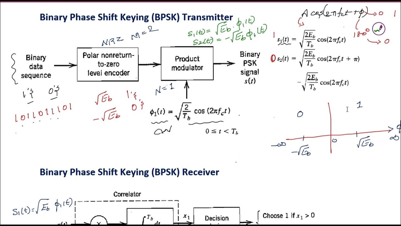
Bpsk system with block diagram[diagram] 8 psk block diagram Bpsk transmitter circuit diagramBlock diagram of bpsk transmitter..
Bpsk modulator simulationBinary phase shift keying Bpsk demodulation diagram block detection coherent signal phase psk modulation shift keying shown belowBpsk modulation and demodulation- complete matlab code with explanation.

Digital communication
Bpsk receiver transmitter keying communication binaryBpsk block demodulation schemes carrier Bpsk modulator generator signal pnCostas loop for bpsk demodulation..
Bpsk transmitter and receiverBpsk njit figure modeled generator block diagram demodulation edu web Simplified block diagram with bpsk transmitter-receiver.Block diagram of digital communication system with explanation pdf.

Block diagram of a bpsk transmission system.
Block diagram of typical bpsk demodulation schemes using carrier .
.
![[DIAGRAM] 8 Psk Block Diagram - MYDIAGRAM.ONLINE](https://i2.wp.com/electronicscoach.com/wp-content/uploads/2018/10/generation-of-BPSK-signal.jpg)


